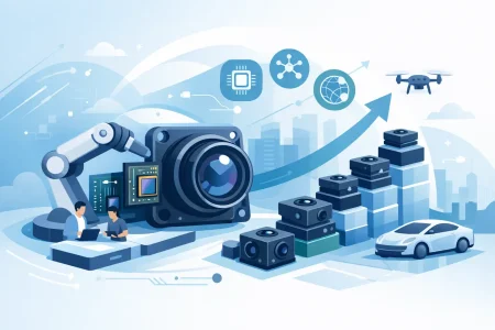

When a camera design stalls at the interface level, the issue is rarely the sensor alone. It is usually the system trade-off behind it – board space, processor compatibility, bandwidth margin, EMI risk, power budget, and how quickly the product needs to move from prototype to production. That is why the dvp vs mipi interface question matters early, not after the hardware stack is already fixed.
For embedded vision products, both interfaces are still relevant. DVP remains practical in cost-sensitive and legacy-friendly designs. MIPI has become the default path for compact, higher-resolution, higher-frame-rate systems. The right choice depends less on trend and more on what your processor, enclosure, image pipeline, and production target can support without compromise.
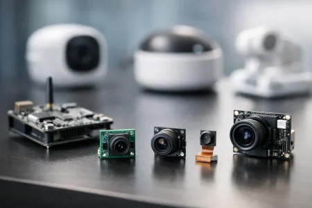
DVP vs MIPI interface at a glance
DVP, or Digital Video Port, is a parallel camera interface. It typically uses multiple data lines plus synchronization and clock signals to move image data from the sensor to the host processor. It is straightforward, widely understood, and still common in many MCU- and DSP-based platforms.
MIPI, usually referring to MIPI CSI-2 in camera applications, is a serial high-speed interface designed for mobile and embedded imaging. It transfers data over differential lanes, reducing pin count while supporting significantly higher throughput. Most modern application processors, SoCs, and AI platforms are built around it.
At a basic level, DVP is easier to understand electrically, while MIPI is more efficient and scalable. That sounds simple, but the engineering decision is not. A low-resolution industrial reader with a stable legacy processor may benefit from DVP. A compact robotics product pushing 4K or multi-camera data almost certainly needs MIPI.
Signal architecture and hardware impact
The biggest physical difference in a dvp vs mipi interface comparison is how data travels across the board.
DVP uses parallel signaling. That means more pins, more traces, and more routing complexity as resolution or bus width increases. An 8-bit or 10-bit data bus can quickly consume valuable connector and PCB resources. As trace count rises, so do timing concerns, especially when the sensor and processor are not placed close together.
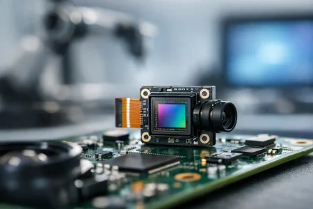
MIPI uses high-speed differential pairs. With fewer signal lines, the connector can be smaller and the flex cable simpler. That is a major advantage in space-constrained products such as handheld medical devices, compact robotics, wearable systems, smart locks, and edge AI cameras. Fewer active lines also help reduce connector size and mechanical complexity.
But MIPI is not automatically easier. The routing rules are tighter. Impedance control, lane matching, stack-up discipline, and signal integrity management matter more. Teams without high-speed layout experience can lose time here. DVP may look bulky, but it can be more forgiving during early development if the data rate is modest.
Bandwidth, resolution, and frame rate
This is where MIPI usually separates itself.
DVP works well when image data volume is moderate. VGA, 720p, and certain 1080p implementations can be viable depending on bit depth, frame rate, and processor capability. Once bandwidth climbs, DVP becomes harder to sustain cleanly. The parallel bus increases routing burden, and the host side may become the bottleneck.
MIPI was built for higher throughput. It supports modern resolutions, higher frame rates, and more advanced image streams with better efficiency. If the design requires 1080p at higher fps, 2MP to 13MP integration, or multiple cameras feeding a processing platform, MIPI is usually the stronger engineering choice.
This matters in commercial products because interface margin affects more than image quality. It affects thermal design, processing load, system stability, and future upgrade paths. A platform that barely supports today’s image stream may block tomorrow’s sensor refresh.
Power consumption and EMI behavior
Power and electromagnetic performance can change the final decision, especially in regulated or noise-sensitive equipment.
DVP’s multiple single-ended lines switch in parallel, which can raise EMI concerns and increase power usage as bus activity rises. In tightly packed systems, that can complicate compliance work and board-level optimization. The wider interface can also increase crosstalk risk if routing is not carefully managed.
MIPI’s differential signaling is generally better suited for lower-power, lower-noise data transfer at high speed. That makes it attractive for battery-powered products and dense embedded assemblies. In many designs, it helps reduce overall interface overhead while supporting better electromagnetic behavior.
That said, MIPI is not immune to problems. If the layout, cable, connector, or termination strategy is poor, signal integrity issues appear quickly. The benefit is real, but only when the implementation is disciplined.
Processor compatibility often decides the answer
In many projects, the interface decision is less about preference and more about host support.
If your processor only exposes a parallel camera input, then DVP may be the practical path unless you add a bridge chip. That can increase BOM cost, board area, software effort, and validation time. On the other hand, if your SoC is built around MIPI CSI-2, forcing a DVP sensor into the architecture can create unnecessary friction.
This is especially common in product redesigns. A team may want to reuse an older DVP camera module for cost or familiarity, but the new platform uses an AI processor with MIPI-only input. At that point, the cheapest sensor is not always the lowest-cost system choice.
For OEMs and device makers, interface alignment should be checked together with ISP path, driver support, operating system requirements, and future sourcing options. A technically compatible camera that slows software bring-up is rarely the best procurement decision.
Cost is more than the module price
DVP camera modules can look attractive from a unit-cost perspective, particularly in mature, lower-resolution designs. The ecosystem is familiar, and integration with older embedded hardware may be straightforward. If the product has a long life cycle and stable specifications, DVP can still be commercially efficient.
MIPI modules may carry a higher integration bar, but they often reduce system cost elsewhere. Smaller connectors, fewer pins, better suitability for compact FPC designs, and easier scaling to newer sensors can offset the initial complexity. In high-volume products, these savings can become significant.
The more useful question is not “Which interface is cheaper?” It is “Which interface lowers total development and production cost for this product class?” That answer changes depending on the processor, target image quality, enclosure limits, and manufacturing scale.
When DVP is still the right choice
DVP remains relevant in embedded systems where simplicity, legacy compatibility, and moderate imaging performance are enough. It fits well in basic industrial inspection tools, entry-level smart devices, barcode readers, educational devices, and long-running platforms built around established processors.
It can also be a smart choice when engineering teams need faster evaluation on known hardware and do not need high-bandwidth image transfer. In these cases, DVP may shorten early bring-up and reduce design risk.
The constraint is growth. If the roadmap includes higher resolution, better frame rates, smaller form factors, or AI processing upgrades, DVP can become the limitation earlier than expected.
When MIPI is the better long-term platform
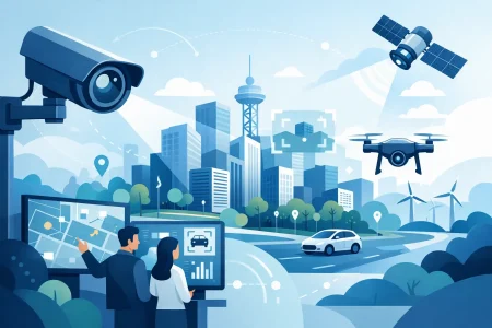
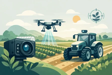
MIPI is usually the stronger option for modern embedded vision products with performance targets beyond basic imaging. It is well suited for medical devices, robotics, smart city systems, driver monitoring, advanced security terminals, and AI-enabled industrial equipment.
It also supports the direction most processor vendors and sensor suppliers are already following. That matters for availability, upgrade flexibility, and long-term design reuse. For businesses planning multiple SKUs or future sensor improvements, MIPI often gives a more scalable platform.
Manufacturers that support both standard and customized camera modules can help reduce the complexity here. For example, when teams need a specific sensor, lens stack, FPC shape, connector orientation, or board-to-board integration strategy, the interface decision becomes part of a larger manufacturability discussion rather than a standalone spec check.
How to choose between DVP and MIPI
Start with the host processor. If the processor strongly favors one interface, that should shape the rest of the decision. Then verify image bandwidth requirements, board space, power targets, cable length limits, EMI constraints, and whether the product roadmap may demand a higher-performance sensor later.
If your design is compact, performance-driven, and intended for future upgrades, MIPI is usually the safer investment. If your design is stable, moderate in bandwidth, and tied to a parallel-input platform, DVP may be the more efficient answer.
For many buyers, the best path is to evaluate the camera module and the host architecture together rather than sourcing them separately. That approach reduces rework, shortens validation, and gives purchasing teams a clearer view of total risk.
A strong imaging product is not built by choosing the newest interface by default. It is built by choosing the one that keeps the sensor, processor, mechanics, and manufacturing plan working together without waste. If the interface decision is made with that discipline, the rest of the camera integration tends to move much faster.