
A camera sensor may advertise a 2-lane or 4-lane MIPI output, while the application processor datasheet lists an MIPI CSI-2 receiver. That looks compatible on paper, but it is not enough to release a board. When engineers ask, “are MIPI lanes compatible,” the practical answer is: only when the electrical PHY, protocol, lane configuration, bandwidth, pinout, and software path all align.
For OEM camera projects, MIPI compatibility must be evaluated as a complete interface chain. A mismatch can cause no image output, unstable streaming, frame corruption, poor electromagnetic performance, or an integration schedule that slips while teams debug hardware and drivers. The fastest path is to verify compatibility before selecting the sensor, camera module, FPC cable, connector, and host platform.
Are MIPI Lanes Compatible Across Different Devices?
MIPI lanes are not universal, interchangeable signal wires. In most embedded camera applications, the term refers to MIPI CSI-2 data lanes and clock signaling between an image sensor or camera module and a processor, ISP, FPGA, or bridge IC. The lane count is only one parameter.
A 2-lane camera module can often connect to a 4-lane CSI-2 receiver if the receiver supports a 2-lane operating mode and the board routes the selected lanes correctly. The unused receiver lanes remain inactive. However, a 4-lane sensor cannot simply be attached to a 2-lane receiver and expected to run at its intended frame rate. Some sensors can be configured for fewer lanes at a higher per-lane data rate, but only if both the sensor and receiver support that rate and the system has enough signal-integrity margin.
Compatibility also depends on whether both ends use the same physical-layer standard. MIPI D-PHY and MIPI C-PHY are different PHYs. They should not be treated as pin-compatible alternatives, even though both may carry CSI-2 camera traffic. A D-PHY sensor requires a D-PHY-capable receiver; a C-PHY sensor requires C-PHY support. Adapter cables do not convert one PHY into the other.
The Six Checks That Determine MIPI Compatibility
1. CSI-2 protocol support
The first requirement is that the transmitter and receiver support compatible CSI-2 operation. Confirm supported CSI-2 versions, packet formats, data types, virtual channels, embedded-data handling, and error reporting. Most standard raw Bayer camera modules use common RAW8, RAW10, or RAW12 formats, but support at the host side can still vary.
This is especially relevant when a design uses HDR sensors, multi-exposure output, stereo cameras, metadata lines, or multiple cameras on one receiver. A host may have enough physical lanes but lack the virtual-channel or ISP support required for the selected sensor mode.
2. D-PHY or C-PHY electrical interface
D-PHY is common in compact camera modules and is based on differential clock and data lane pairs. A typical D-PHY camera uses one differential clock pair plus one, two, or four differential data pairs. C-PHY uses three-wire trios and a different signaling method.
Check the host datasheet for the exact supported PHY type, number of lanes or trios, minimum and maximum lane rate, termination requirements, and clocking restrictions. Do not assume that a processor with “MIPI CSI” in its feature list supports every MIPI camera interface available in the market.
3. Lane count and lane mapping
Lane count affects bandwidth, but the physical mapping must also be correct. Many camera modules use FPC connectors with a manufacturer-specific pin sequence. Two modules may both have 24-pin FPC connectors, yet assign power, ground, I2C control, reset, clock, and CSI-2 lanes to completely different pins.
Lane polarity matters as well. Some receivers allow P/N polarity inversion through configuration, while others do not. Lane swapping may be permitted by a processor or FPGA, but it must be verified at both the hardware and software levels. A connector that fits mechanically is never proof of electrical compatibility.
4. Available bandwidth at the required image mode
A camera link must carry the active resolution, frame rate, pixel format, blanking overhead, and any embedded data. A useful early estimate is:
Required throughput = horizontal pixels × vertical pixels × frames per second × bits per pixel, plus protocol and timing overhead.
For example, a 1920 × 1080 sensor operating at 60 fps in RAW10 generates about 1.24 Gbps of active pixel data before overhead. A 2-lane D-PHY interface may support the mode if each lane can run at the required rate, but the exact result depends on sensor timing and host receiver limits.
More lanes do not automatically improve image quality. They provide additional transport capacity or allow the same data rate to be distributed across lanes at a lower per-lane speed. For a compact, low-power design, a 2-lane solution may be the better engineering choice. For high-resolution, high-frame-rate machine vision or multi-camera applications, 4 lanes can provide the necessary margin.
5. Clocking, timing, and control signals
The CSI-2 link is only part of the camera interface. The sensor may require an external master clock, typically called MCLK or XVCLK, with specific frequency accuracy and jitter limits. It also needs stable power rails in the correct sequencing order, reset and standby control, and an I2C or I3C control connection for register configuration.
A module can have compatible MIPI lanes and still fail because the host does not provide the required clock frequency, reset timing, or voltage levels. I2C address conflicts can also appear when integrating multiple cameras. These details should be reviewed before schematic completion, not after prototype assembly.
6. Software, drivers, and ISP support
Hardware compatibility does not guarantee that the operating system will detect or stream from the camera. The host needs a sensor driver, proper device-tree or board configuration, clock definitions, lane settings, and a supported media pipeline. The ISP must also accept the sensor’s raw format and operating modes if image processing is performed on the host.
For Linux-based embedded systems, verify the V4L2 driver path, media-controller topology, and supported sensor modes. For Android, confirm the camera HAL and tuning requirements. FPGA-based systems need CSI-2 receiver IP, PHY configuration, packet handling, and a downstream image-processing architecture.
PCB and FPC Design Can Change the Result
At MIPI data rates, correct routing is part of interface compatibility. Differential pairs need controlled impedance, matched intra-pair lengths, continuous reference planes, and limited discontinuities. Stubs, poor connector selection, excessive FPC length, sharp routing changes, and weak grounding can degrade the eye margin even when the schematic is correct.
A production camera module should be selected with its mechanical integration in mind. The sensor orientation, module thickness, lens height, FPC bend radius, connector position, and cable length all influence the final product design. Industrial and medical equipment may also need additional attention to EMC performance, temperature range, vibration, and repeated cable movement.
For short board-to-board connections, a standard MIPI FPC module can be highly efficient. For longer distances, designers may need a serializer-deserializer architecture rather than attempting to extend raw MIPI lanes beyond their practical routing range. This changes the interface strategy and should be decided early in the system architecture.
A Practical Compatibility Review Before Ordering Samples
A disciplined review avoids expensive rework. Start with the processor or FPGA receiver specifications, then define the target resolution, frame rate, pixel format, and image-quality requirements. Select a sensor mode that fits the receiver’s lane-rate and lane-count limits with realistic margin.
Next, compare the camera module’s connector pinout, power rails, MCLK requirement, control interface, reset behavior, and mechanical envelope against the carrier board. Confirm that the required driver and ISP support are available for the chosen host platform. If the project uses a custom lens, infrared filter, FPC length, housing, or mounting geometry, validate these changes alongside the electrical design rather than treating them as separate tasks.
For high-volume products, prototype evaluation should include image testing, stream stability, thermal behavior, ESD performance, and manufacturing repeatability. A module that works on an engineering bench but has narrow signal margin can become a costly production issue.
When a Custom MIPI Camera Module Is the Better Choice
Standard modules reduce development time when their sensor, connector, FPC, and optical stack already match the product. Custom development becomes more valuable when the application has a strict mechanical envelope, unusual cable routing, low-light requirement, fixed-focus distance, medical or industrial reliability target, or a specific processor platform.
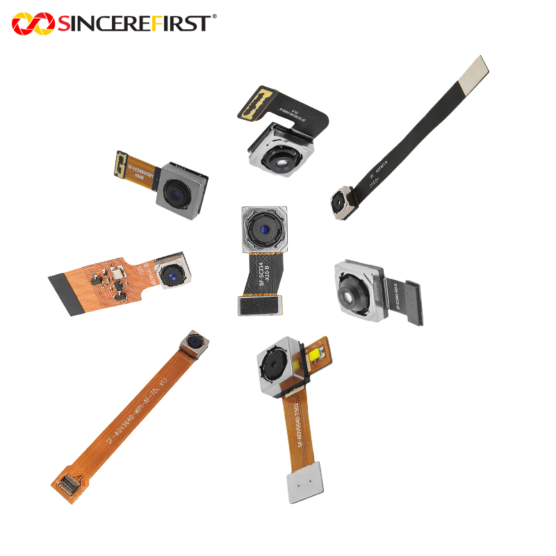
SincereFirst supports MIPI camera module selection and customization from sensor and lens matching through FPC design, connector definition, and scalable manufacturing. For procurement and R&D teams, the key benefit is not simply obtaining a camera with the right lane count. It is receiving a module engineered around the actual host, optical requirement, and production constraints.
The right question is not whether two MIPI lane counts look similar. It is whether the complete camera interface has been designed to operate reliably at the required image mode, across every unit that reaches production.