
A sensor decision made early in a camera program can determine far more than image quality. It influences module size, power budget, interface selection, illumination design, production cost, and even whether a device can meet its intended frame rate. For product teams evaluating CMOS versus CCD imaging, the practical question is not which technology is universally better. It is which sensor architecture produces dependable image data under the actual conditions of the finished device.
CCD sensors established the benchmark for scientific and professional imaging over many years. CMOS technology has since become the dominant choice in embedded cameras, mobile devices, machine vision, and many medical and industrial systems. That shift reflects significant advances in CMOS pixel design, readout speed, low-light performance, and integrated processing.
CMOS Versus CCD Imaging at the Sensor Level
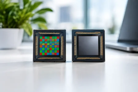
Both CMOS and CCD image sensors convert photons into electrical signals. Their primary difference is how they move and read those signals.
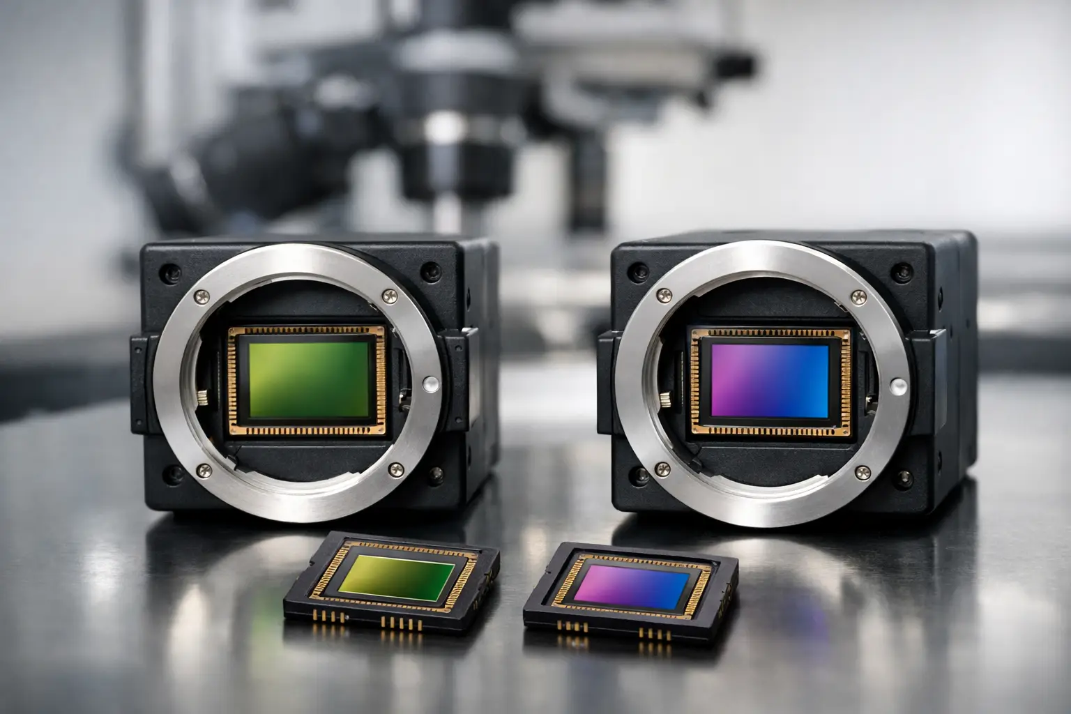
In a CCD, or charge-coupled device, charge generated by each pixel is transferred across the sensor to one or a small number of output amplifiers. This shared readout structure can provide highly uniform output and low noise, particularly in carefully controlled exposure conditions. Historically, those qualities made CCD sensors a strong choice for scientific cameras, astronomy, microscopy, and inspection tasks where image consistency outweighed speed and system cost.
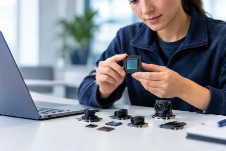
A CMOS, or complementary metal-oxide-semiconductor, sensor typically includes active circuitry at the pixel level. Pixels can be addressed and read through column-parallel circuitry, allowing much faster data extraction. CMOS sensors can also integrate analog-to-digital conversion, timing control, image processing functions, and power-management features directly on the chip.
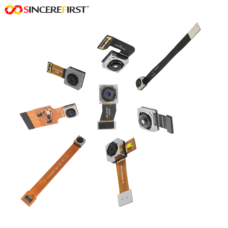
For an embedded device manufacturer, that integration matters. It can reduce supporting electronics, simplify a camera module design, lower power consumption, and support compact interfaces such as MIPI CSI-2. Modern CMOS sensors are therefore available across a wide range of resolutions, pixel sizes, frame rates, and optical formats.
Why CMOS Has Become the Default for New Designs
CMOS is now the practical default for most new camera module projects because it aligns well with the commercial requirements of intelligent hardware. Robotics, smart retail terminals, access-control products, agricultural equipment, security cameras, and portable medical devices often need small form factors, rapid image capture, low heat generation, and a stable supply path at volume.
Speed is one major advantage. CMOS sensors can support high frame rates and rapid region-of-interest readout, which are valuable for barcode recognition, motion analysis, robotic guidance, and high-speed inspection. A system does not always need to read every pixel at every cycle. With the right sensor and firmware, a design can prioritize the image area that drives the decision.
Power efficiency is another advantage. Battery-operated products and compact enclosures have limited thermal capacity. A lower-power sensor architecture can ease thermal design and extend operating time, while helping preserve image stability in enclosed equipment.
CMOS manufacturing also benefits from broad semiconductor ecosystem support. This has helped expand sensor selection and reduce cost across mainstream resolutions. For OEM programs that require a long production run, supplier qualification should still examine sensor lifecycle status, lot consistency, and availability of compatible components. Low unit cost alone is not a reliable indicator of long-term sourcing security.
CMOS limitations to engineer around
CMOS performance is not identical across all sensors. Low-cost devices may show higher fixed-pattern noise, reduced dynamic range, weaker low-light performance, or rolling-shutter distortion. These characteristics are not reasons to reject CMOS. They are design inputs that must be matched to the application.
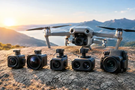
Rolling shutter is particularly relevant when the object or camera moves quickly. Because rows are exposed and read at slightly different times, fast motion can make straight edges appear skewed or stretched. For industrial automation, drone imaging, high-speed conveyors, and moving robotic arms, a global-shutter CMOS sensor is often the appropriate answer. It captures the full image frame at the same instant, reducing motion artifacts.
Where CCD Still Makes Sense
CCD technology remains relevant in specialized imaging systems, especially where its characteristics are already validated and the operating environment is tightly controlled. Certain legacy scientific instruments, high-end microscopy platforms, and long-exposure applications may continue to use CCD sensors because of established optical designs, proven calibration methods, or specific noise behavior.
CCD sensors can offer excellent image uniformity and high sensitivity in some use cases. Their charge-transfer approach has historically supported clean images at long exposure times, making them useful when the scene is static and light levels are carefully managed.
The trade-off is system complexity. CCD cameras often need more specialized clocking and analog support circuitry. They can consume more power, generate more heat, and operate at lower frame rates than comparable modern CMOS designs. They are also generally less aligned with the compact, high-volume module formats used in current embedded products.
For a new commercial design, selecting CCD should be a deliberate technical decision supported by measurable image requirements, not an assumption that CCD automatically delivers better quality. A well-selected CMOS sensor often outperforms an older CCD option in real-world application results.
Compare the Factors That Affect Your Camera Module
Sensor selection should begin with the image data your system must produce. Resolution is only one part of that requirement. A 12-megapixel sensor does not automatically improve a detection task if the lens, illumination, working distance, processing bandwidth, or target size cannot use the added pixels.
Start with shutter type and scene movement. A rolling-shutter CMOS sensor is efficient and economical for static documents, fixed security views, patient monitoring, and many consumer devices. A global-shutter CMOS sensor is better suited to fast industrial movement, gesture recognition, machine guidance, and automated optical inspection.
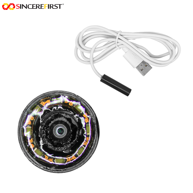
Next, evaluate sensitivity and pixel size. Larger pixels generally collect more light, but sensor format, quantum efficiency, noise control, and lens aperture all affect final low-light performance. For endoscope modules, medical imaging systems, and compact inspection probes, optical constraints can be as decisive as the sensor specification. A small sensor may require precise lens selection, controlled LED illumination, and careful signal tuning to achieve usable images.
Dynamic range is equally important where a scene contains bright reflections and dark detail. Metal parts, vehicle plates, outdoor entrances, and surgical environments can all create challenging contrast. High dynamic range CMOS sensors may preserve more usable information in these scenes, but the result should be confirmed through sample images under representative lighting.
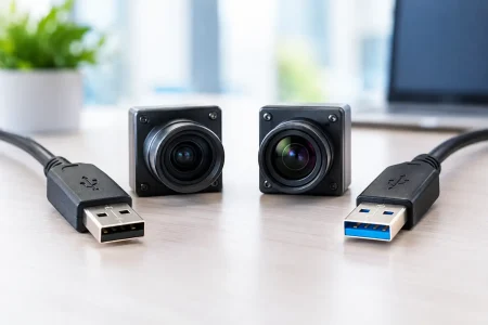
Finally, consider output interface and processing load. MIPI camera modules are well suited to compact embedded boards with compatible application processors. USB 2.0, USB 3.0, and UVC modules can simplify integration for PCs, industrial controllers, and rapid prototypes. The sensor must match the bandwidth of the chosen interface, and the host platform must be able to receive, process, and store the intended image stream without dropped frames.
Validate the Complete Imaging Chain
A sensor comparison based only on a datasheet can lead to expensive redesigns. The final image depends on the complete chain: sensor, lens, infrared filter, illumination, mechanical alignment, cable length, interface, firmware, image signal processor settings, and host software.
A practical evaluation should use the actual target, working distance, motion speed, lighting angle, and enclosure conditions. Test for exposure stability, color reproduction where relevant, sharpness at the field edges, noise in low light, motion artifacts, and thermal behavior during extended operation. For production equipment, teams should also assess module-to-module variation and image consistency across sample lots.
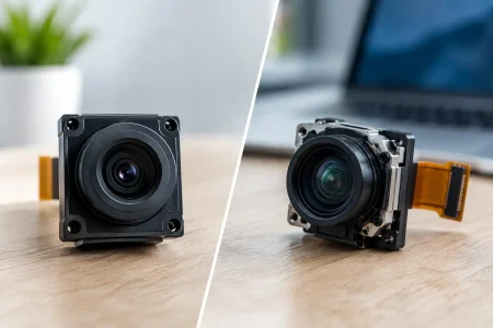
Customization is frequently required at this stage. A standard camera module may need a different lens field of view, fixed-focus distance, FPC length, connector orientation, IR-cut configuration, LED arrangement, or housing geometry. These changes should be engineered as part of the imaging solution rather than treated as late mechanical adjustments.
Choose for the Product Lifecycle, Not Just the Prototype
The best sensor is the one that keeps delivering usable image data after the product moves from laboratory testing to volume manufacturing. That means balancing image performance with component availability, manufacturability, calibration needs, regulatory requirements, and total system cost.
For most new embedded vision programs, CMOS provides the strongest combination of speed, integration, power efficiency, and scalable supply. CCD remains a valid option when a specialized application has proven reasons to require it. The disciplined approach is to define the image task first, validate modules in the real environment, and work with an engineering partner that can adapt optics, electronics, and production controls as the design matures.
SincereFirst helps OEMs move from sensor selection to production-ready camera modules with the technical customization and manufacturing discipline that intelligent imaging products require.