
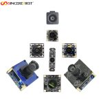
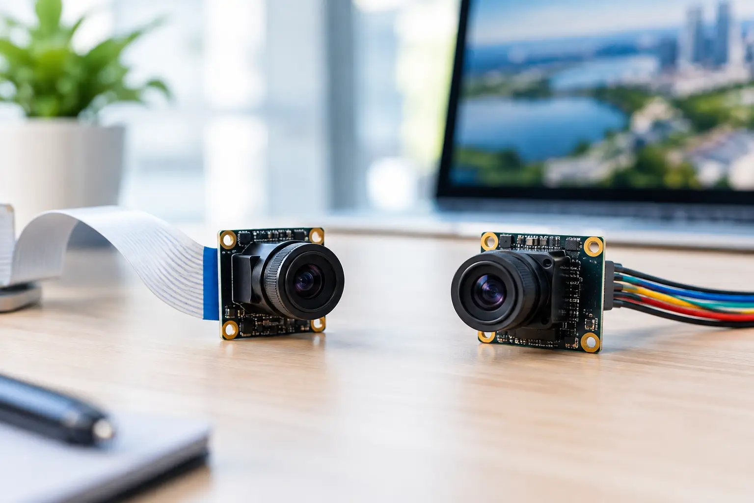
A camera interface choice can determine whether a compact vision product reaches production on schedule or enters another PCB revision cycle. In the MIPI CSI-2 versus DVP decision, the sensor is only one part of the equation. Processor support, cable length, resolution, frame rate, board area, power budget, and manufacturing test method all affect the right answer.
For most new high-resolution embedded designs, MIPI CSI-2 is the forward-looking interface. DVP remains a practical and economical option where the host processor already supports it, image data rates are modest, and design simplicity outweighs long-term interface scalability. The best selection comes from matching the module, host, and final product requirements rather than choosing the newest protocol by default.
MIPI CSI-2 versus DVP: The Core Difference
DVP, also called a parallel camera interface, sends pixel data over multiple parallel data lines. A typical implementation uses 8, 10, or 12 data bits plus pixel clock, horizontal synchronization, vertical synchronization, power, ground, and control lines such as I2C. The receiver samples all data bits at the same time on each clock edge.
MIPI CSI-2 serializes image data into packets and transmits it over one or more high-speed differential lanes. Most camera modules use the MIPI D-PHY physical layer, with a clock lane and one to four data lanes. CSI-2 can also operate with C-PHY in supported systems, but D-PHY remains the common choice for embedded camera modules and application processors.
This architectural difference drives nearly every practical trade-off. DVP is easy to understand and debug at lower speeds, but it consumes many pins and becomes difficult to route as throughput rises. MIPI CSI-2 reduces pin count and supports substantially higher bandwidth, but it requires a host with compatible CSI-2 hardware and careful high-speed layout.
Bandwidth Sets the First Boundary
Image data volume rises quickly with resolution, bit depth, frame rate, and the selected output format. A 2-megapixel camera at 30 frames per second may be comfortable on either interface, depending on pixel format and host capability. A 5MP, 8MP, or higher-resolution sensor running at real-time frame rates usually favors MIPI CSI-2.
DVP transfers several bits every pixel clock cycle. As the pixel clock increases, clock-to-data skew becomes more difficult to control. Each trace must arrive at the receiver within a narrow timing window. Board routing, connector variation, FPC length, and signal reflections can all reduce margin.
CSI-2 replaces the wide parallel bus with differential high-speed lanes. This approach carries more data with fewer conductors and is better suited to compact products using modern mobile, AI, and industrial processors. It also supports packet features such as multiple virtual channels, which can be useful for multi-camera systems or sensors that output separate image streams and metadata.
Higher interface bandwidth does not automatically mean better images. If the host ISP cannot process the selected sensor mode, or if memory bandwidth is insufficient, a faster interface will not solve the system bottleneck. Evaluate the full image pipeline: sensor output, interface receiver, ISP, DDR bandwidth, encoder, AI accelerator, and storage or network path.
Pin Count, Board Area, and Mechanical Integration
DVP can require more than a dozen high-speed-related signals once data lines, synchronization signals, clocks, and controls are counted. That may be acceptable on a larger industrial controller with a short board-to-board connection. It is much less attractive in a battery-powered handheld device, slim smart terminal, compact robot, or medical instrument.
A two-lane MIPI CSI-2 camera commonly uses fewer high-speed conductors while providing greater throughput than a comparable DVP implementation. Fewer conductors can reduce connector size and FPC width, giving mechanical teams more freedom around batteries, displays, enclosures, and thermal parts.
The benefit should be assessed realistically. CSI-2 lowers signal count, but its differential pairs need controlled impedance, appropriate spacing, continuous reference planes, and lane-length matching. A well-executed MIPI design is compact and efficient. A poorly routed MIPI design can create intermittent capture failures that are expensive to isolate late in validation.
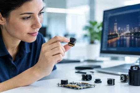
For custom camera module projects, the mechanical interface matters as much as the electrical standard. Lens height, module thickness, FPC bend direction, connector position, shielding, and cable length should be reviewed before the interface is finalized. Changing from DVP to MIPI after enclosure tooling has started may affect more than the PCB.
Host Processor Support Is Often the Deciding Factor
The host platform should be checked before selecting a sensor or camera module. Many current application processors, system-on-chips, and AI platforms include dedicated MIPI CSI-2 receiver ports and ISP support. Some microcontrollers and older processors offer only a parallel camera input, or support MIPI only through an external bridge.
If a processor natively accepts DVP and the product needs VGA, 720p, or another moderate-throughput mode, DVP may shorten development. There is little commercial value in adding a bridge IC, additional power rails, and firmware complexity solely to force a MIPI module into a DVP-only platform.
Conversely, using a high-resolution DVP sensor with a processor optimized for CSI-2 often creates avoidable risk. An external parallel-to-CSI bridge can add cost, latency, board area, power consumption, and supply-chain dependencies. When a product roadmap includes higher resolution or multiple cameras, a native CSI-2 host interface is generally the more scalable foundation.
Ask the processor supplier or board team for exact receiver details, not only a generic statement that the chip supports cameras. Confirm the number of CSI ports, available lane count, maximum lane rate, supported data types, virtual channel capability, ISP sensor drivers, and whether the required sensor mode has been validated.
Signal Integrity and PCB Design Requirements
DVP layout focuses on matching data-line timing to the pixel clock, controlling trace length, minimizing stubs, and maintaining clean power delivery. It is a familiar interface for many engineering teams, especially in legacy embedded products. At higher pixel clocks, however, the wide bus increases routing congestion and timing sensitivity.
MIPI CSI-2 requires differential impedance control and disciplined routing of each lane pair. Designers should keep pairs tightly coupled, avoid unnecessary vias, maintain a stable ground reference, and follow the host processor’s layout guidance for skew, trace length, and termination. Clock and data lanes must also be assigned exactly as required by the receiver.
Cable selection deserves equal attention. A short FPC between a camera module and main board is common, but longer flex assemblies can introduce insertion loss and electromagnetic susceptibility. For a moving robot arm, endoscope subsystem, or industrial device with repeated flexing, the interconnect must be evaluated for both signal performance and mechanical life.
Laboratory validation should include more than a successful image preview. Test every intended resolution and frame rate across temperature, supply variation, cable tolerance, and repeated power cycles. Capture stability, lane errors, frame drops, startup behavior, and electromagnetic performance need documented acceptance criteria before volume production.
Power, Cost, and Production Considerations
MIPI CSI-2 is frequently associated with lower power because it uses low-voltage differential signaling and can move high data rates efficiently. Actual system power depends on sensor mode, lane rate, host receiver behavior, ISP load, display or encoding workload, and software settings. A lower-resolution DVP design can consume less total power than a high-frame-rate MIPI design simply because it processes less image data.
DVP can reduce cost when the host already includes a parallel receiver and the camera module is a standard configuration. Its larger connector and extra PCB routing may offset some savings in compact products. MIPI CSI-2 modules are widely available across modern sensor families, but the total cost should include high-speed PCB requirements, connector selection, validation effort, and firmware development.
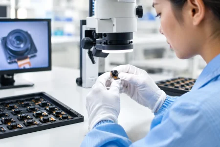
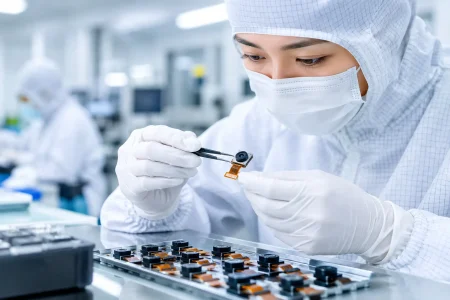
Production repeatability is another consideration. Camera modules need stable FPC specifications, connector mating force, optical alignment, image tuning, and electrical test coverage. For OEM programs, a supplier should be able to verify interface function at the intended operating mode, maintain component traceability, and control changes to sensor, lens, and flex components.
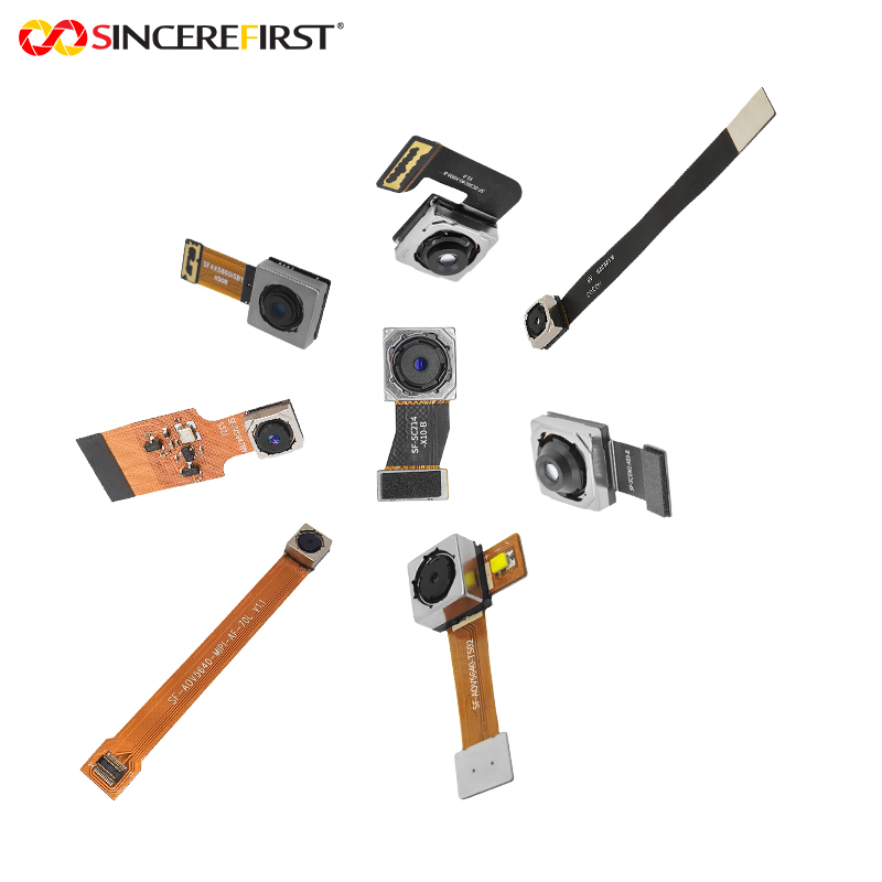
SincereFirst supports both MIPI and DVP camera module development, allowing product teams to select the interface that fits their host platform rather than adapting the product around a limited module range. For specialized applications, custom FPC length, connector type, sensor selection, lens field of view, module dimensions, and image tuning should be defined early alongside the interface requirement.
A Practical Selection Method
Start with the required image output: resolution, frame rate, pixel format, bit depth, latency, and number of cameras. Then verify what the host can receive and process. These two steps eliminate many unsuitable options before schematic work begins.
Choose DVP when the platform has a native parallel input, required bandwidth is moderate, the interconnect is short, and a simple established design has more value than interface headroom. Choose MIPI CSI-2 when product size is constrained, resolution or frame rate is high, the host provides native CSI-2 ports, or the roadmap may add cameras and higher-performance sensors.
The most productive next step is to provide the camera supplier with the host processor model, target sensor mode, mechanical envelope, FPC length, operating environment, and annual volume estimate. With those details defined, interface selection becomes an engineering decision with measurable margins, not a late-stage compatibility gamble.