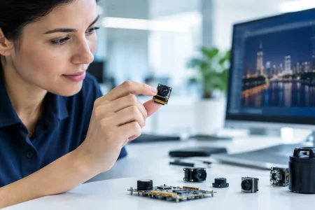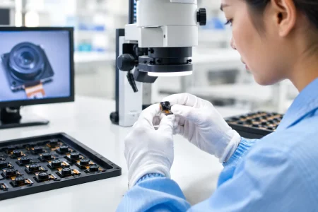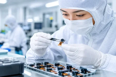

A missed scratch on a reflective housing, a blurred code on a fast conveyor, or an invisible contaminant on a food line can turn a camera specification into a costly production problem. Selecting the best imaging sensors for industrial inspection starts with the defect, material, motion, and measurement tolerance – not with resolution alone.
For OEMs, machine builders, and system integrators, the right sensor is the one that produces stable, repeatable image data under actual line conditions. That decision must account for illumination, lens design, triggering, processing bandwidth, enclosure limits, and long-term module availability. A high-resolution sensor can still be the wrong choice if its rolling shutter distorts moving parts or its sensitivity forces excessive exposure time.
What Defines the Best Imaging Sensors for Industrial Inspection?
Industrial inspection generally favors CMOS sensors because they offer fast readout, low power consumption, compact module integration, and broad resolution choices. But “CMOS” is only the starting point. A sensor should be evaluated against the smallest defect that must be detected, the field of view, the object speed, the working distance, and the contrast available between the defect and its background.
Pixel count matters when inspection requires spatial detail across a wide field of view. If a system must identify a 0.1 mm defect across a 300 mm web, the required pixel density may be substantial. However, increasing resolution also increases data throughput, processing demand, lens requirements, and often system cost. If the inspection station only needs to confirm the presence and orientation of a component, a lower-resolution sensor with faster frame rate and better low-light behavior may deliver more dependable results.
The practical goal is not to buy the largest sensor or the highest megapixel count. It is to create sufficient pixels on the target defect, with enough contrast and repeatability to support the pass/fail decision.
Global Shutter Sensors for Motion-Critical Lines
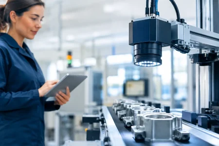
Global shutter CMOS sensors expose every pixel at the same instant. They are typically the first choice for moving production lines, robotics, pick-and-place verification, high-speed packaging, electronics assembly, and code reading on fast parts.
With a rolling shutter, pixels are exposed line by line. Motion during readout can make circular features appear tilted, stretch printed characters, or shift edges between frames. These artifacts can compromise dimensional measurement and cause unstable machine vision results, even when nominal resolution is adequate.
Global shutter sensors do have trade-offs. Compared with similar rolling shutter designs, they may offer lower resolution options, higher cost, or reduced low-light sensitivity in some configurations. For a stationary inspection fixture or a slow-moving sample under controlled illumination, rolling shutter can be a cost-effective option. For motion where positional accuracy matters, global shutter is usually the safer engineering decision.
Frame Rate Must Match Part Speed
Frame rate is not simply a performance number. It determines whether the camera captures each required inspection position without gaps. A conveyor application may need a moderate frame rate if a photoelectric trigger captures one image per part. Continuous web inspection, by contrast, may require high-speed area scan imaging or a line scan architecture that matches web velocity and encoder feedback.
Exposure time is equally critical. Short exposure freezes motion but reduces collected light. The usual solution is not to accept a noisy image – it is to design appropriate strobed illumination, select a sensor with adequate sensitivity, and synchronize the trigger, light, and camera module.
Pixel Size, Sensitivity, and Noise
Pixel size influences how much light each pixel can collect. Larger pixels often support better sensitivity and signal-to-noise performance, especially in low-light environments or applications requiring short exposure. This can be valuable for warehouse automation, industrial endoscopy, low-light cavity inspection, and high-speed production equipment.
Smaller pixels enable high resolution in a compact optical format. They are well suited to close-range electronics inspection, label verification, precision assembly, and compact smart devices where space is limited. The trade-off is that smaller pixels place greater demands on lighting and lens quality. Poor illumination, low-quality optics, or excessive gain can erase the benefit of a high-pixel-count sensor.
Dynamic range also deserves attention. Inspection targets often include bright metal, dark plastic, glossy coatings, solder joints, and printed markings in the same scene. A sensor with strong dynamic range can preserve detail across these highlights and shadows. Where contrast is especially difficult, controlled lighting, polarizers, multi-exposure capture, or HDR sensor modes may be more effective than resolution upgrades alone.
Spectral Response Should Follow the Defect
Visible-light RGB and monochrome sensors cover most standard inspection tasks, but some defects are not visible in the normal color spectrum. The best sensor choice depends on what creates usable contrast.
Monochrome sensors are often preferred for edge measurement, OCR, code reading, surface texture analysis, and other applications where color information is unnecessary. Without a color filter array, they can provide greater effective detail and sensitivity than comparable color sensors.
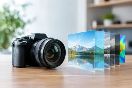
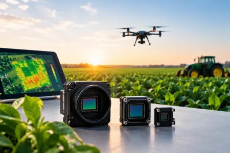
Near-infrared sensors can improve contrast through certain inks, plastics, coatings, and organic materials. They are commonly considered for sorting, agricultural inspection, security-related imaging, and some packaging checks. Ultraviolet imaging can reveal fluorescent coatings, residues, and surface treatments. Short-wave infrared, or SWIR, supports specialized inspection of moisture, fill levels, semiconductor materials, and content hidden by some visible-opaque packaging.
Specialized spectral imaging adds cost and integration complexity. It should be justified by a defect that conventional visible imaging cannot detect reliably. A well-designed visible-light system remains the most efficient solution for many production tasks.
Area Scan or Line Scan?
Area scan cameras capture a complete two-dimensional image in one exposure. They are the standard choice for discrete parts, robot guidance, assembly verification, gauges, labels, and most station-based inspections. Their integration is straightforward when a part can be triggered within a defined field of view.
Line scan sensors capture one line of pixels at a time while the object or camera moves. They are designed for continuous materials and large surfaces, including steel, glass, paper, textiles, film, batteries, and printed webs. By combining successive lines with accurate motion control, a line scan system can inspect long or wide products at very high resolution.
The choice is operational, not theoretical. An area scan sensor is usually simpler for individual products. A line scan sensor becomes necessary when the inspected surface is continuous, very wide, or moving too quickly for a conventional area image to maintain required detail.
Interface Selection Affects System Stability
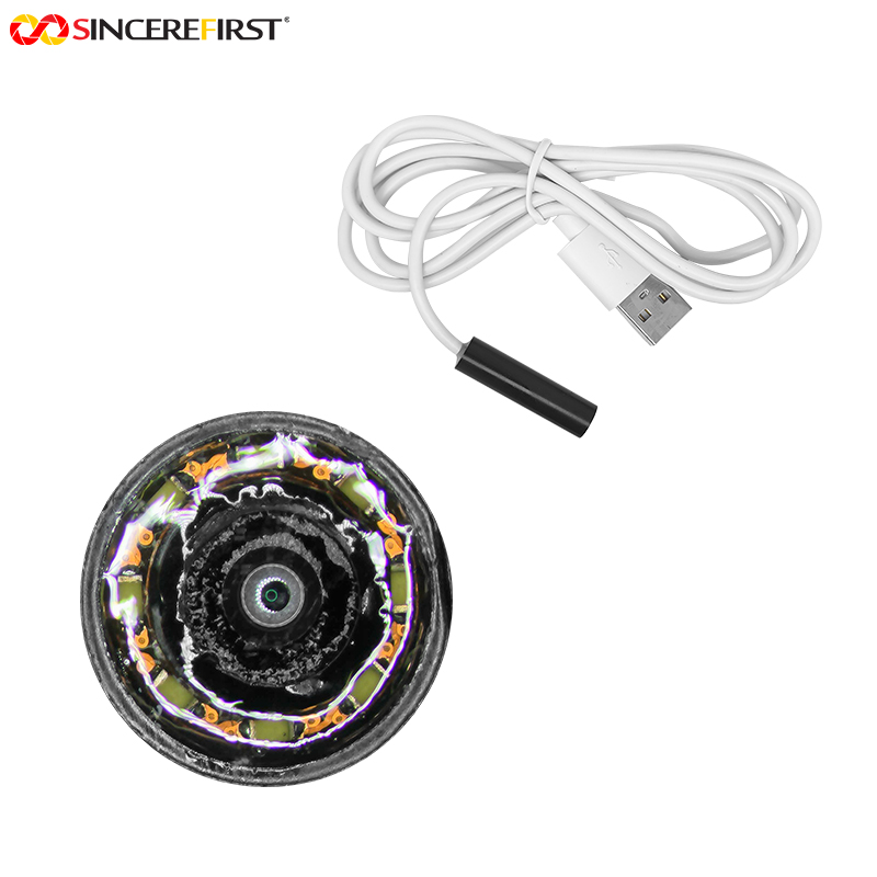
Sensor performance is only useful when image data reaches the host system reliably. USB camera modules are practical for prototypes, compact inspection stations, and systems where plug-and-play UVC compatibility is valuable. USB 3.0 offers materially higher bandwidth than USB 2.0 and is better suited to high-resolution or high-frame-rate imaging.
MIPI CSI-2 modules are a strong fit for embedded Linux and Android platforms, robotics controllers, handheld devices, and space-constrained intelligent equipment. They provide a compact, efficient connection but require careful host compatibility, driver support, cable-length planning, and electromagnetic interference control.
For each interface, confirm not just peak bandwidth but cable routing, connector retention, host processing capacity, power budget, trigger requirements, and expected operating environment. An inspection system on a factory floor needs a stable integration path that can be manufactured repeatedly, not a laboratory setup that works only with short cables and ideal conditions.
Build the Camera Module Around the Inspection Task
The sensor is central, but it is one element in the imaging chain. Lens selection determines field of view, distortion, depth of field, and corner sharpness. Lighting determines contrast. Mechanical design controls focus retention, vibration resistance, thermal behavior, and contamination exposure. Image signal processing can improve usability, but it cannot fully recover information that was not captured at the sensor.
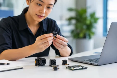
For a custom module, engineering teams should define the target defect size, working distance, field of view, line speed, illumination method, acceptable false-pass rate, enclosure dimensions, interface, and production volume before selecting components. This shortens prototype cycles and reduces the risk of redesign after mechanical integration.
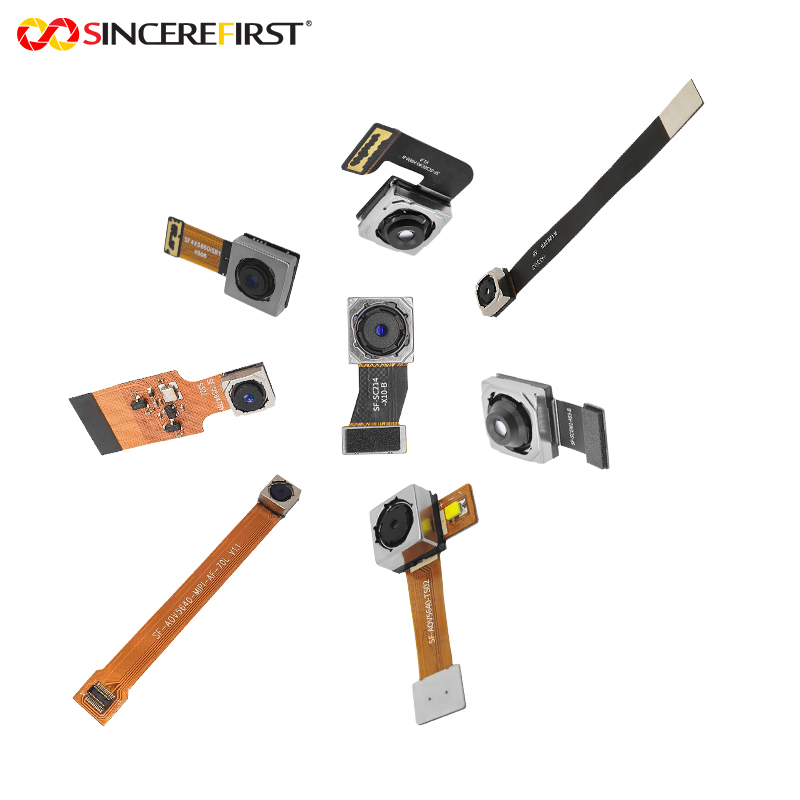
SincereFirst supports this process with standard and customized camera modules across MIPI, USB, DVP, FPC, and specialized imaging configurations. For industrial projects, early alignment between sensor selection, optics, interface, and manufacturing requirements is often what turns a promising proof of concept into a scalable inspection product.
A sensor should earn its place by making the defect clear, the timing repeatable, and production decisions trustworthy. When the imaging chain is specified around those outcomes, inspection equipment can operate with the precision that high-volume manufacturing demands.